![<?echo $_SERVER['SERVER_NAME'];?>](/template/twentyseventeen/skin/images/header.jpg)
Stencil cutting technology
For wafer raised webs, the cutting technique must be able to produce thousands of closely spaced, very small perforations, with extremely high dimensions and position tolerances. Slight deviations from the optimum hole size can also result in large differences in bump height, and in extreme cases lead to open circuit of the assembled and underfill chip. In addition, the location of the perforations must also be maintained as close as possible to the computer-generated design. Since the entire pad on the wafer must be fully printed to obtain an acceptable reflow bump, the space between the perforations must be sufficient to avoid bridging when printing is done under tight pad spacing conditions. defect. Therefore, the distance between the perforations should not be less than 3 mils (in terms of 3 mil thick stencils). In some cases, the perforation needs to be offset, avoiding being placed completely in the center of the pad. Depending on the density of perforations in a particular area of ​​the screen, it may only be necessary to print a portion of the pad. Since the area of ​​the pad on the wafer can be less than 4 mils, the stencil cutting technology must be able to accurately locate the puncture, and the offset can only be less than a few micrometers.
Of the existing technologies in the market, only laser-cut and electroformed stencils are suitable for the reproduction of computer-generated artwork and can meet the requirements for effective wafer printing. Although many different suppliers use the same technology to cut stencils, their capabilities vary. In general, the laser cutting process leaves a rough through the special polishing and plating technology remediation on the perforated wall surface. Another feature of laser cutting is that the perforated wall surface of the screen has a slope, and the opening size of one side of the screen is slightly larger than the other side. Some suggestions are that if larger perforations are at the bottom of the screen, tapered perforations can actually enhance the release of solder paste from the screen. The disadvantage of the laser cutting process is that the cost of producing stencils with innumerable small perforations is high, and the greater the number of perforations, the higher the cost of producing laser-cut stencils. Conversely, the cost of producing an electroformed screen's artwork is independent of the number of perforations designed. The perforation size and position of the electroformed screen is as accurate as the laser-cut screen, and the perforated wall, although not naturally beveled, is relatively smooth.
Stencil thickness
The thickness of the stencil metal foil plays a decisive role in deciding how much perforation is required to apply the amount of solder paste required to achieve the target reflow bump height. According to the wafer bump study, it is recommended that the thickness of the stencil be selected according to this standard: the ratio of the minimum perforated wall area of ​​the stencil to the area of ​​the perforated opening (i.e. area ratio) is less than 1.75.
Perforation size
In the correct stencil design that meets the recommended area ratio of less than 1.75, the stencil thickness and the perforation size are closely related. If the required amount of solder paste is the same, a thinner stencil requires a larger perforation size; thicker dies require a smaller perforation size. For tightly spaced pads, it is sometimes necessary to find the most appropriate combination of hole size and thickness for acceptable transfer efficiency. It is an extremely challenging task to meet the requirements of the amount of solder paste without making the perforation too tight. The biggest stencil design challenge is often in the corners of the die, and this situation is very common. Another important thing to note when designing a beveled laser-cut hole is that it must be kept in mind that the opening area at the bottom of the screen must be larger than at the top, and a larger opening area means that the spacing between the perforations is smaller.
Perforated shape
Filler and release steps in the screen printing process are all affected by the shape of the perforations. To achieve a more consistent and superior filler quality, rounded corners have a better effect than sharp corners because the flow of solder paste through the edges of microbends is far easier than filling in sharp corners, while oval and round Filler effect is much better than triangles and diamonds. However, the round hole piercing has some disadvantages in the release process.
Perforation orientation
The size and geometry of the perforations when designing a robust screen are important considerations, but the effect of the perforation orientation on the distribution of reflow bump sizes cannot be ignored. In addition to filling the maximum amount of solder paste with the highest transfer efficiency, and without causing too much solder paste to fall and causing bridging defects, it is also very important to make the amount of screen printing paste per chip on the wafer consistent. If the height of the protrusion formed by the reflow solder paste is too wide, open or short circuit may occur after assembly. Larger projections may adhere to multiple bond pads or other objects: insufficient protrusion will not adhere to any object. By designing a perforated orientated screen, it is possible to improve the control of the printing accuracy and the distribution of the solder paste coating.
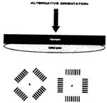
Figure 3: The amount of filled solder paste as per A arrangement may be inconsistent with the arrangement of perforations such as B.
Circular perforations have no orientation problem because any angle is the same for the orientation of the target; but the square is not the case and will become a diamond at 45°. The problems of oval and oblong perforation are more serious because of the different east-west orientation, north-south orientation, or any angular orientation. Screen printing paste fills the perforations differently for perforations of the same size and geometry, but different orientations. To achieve consistent packing and release, it is best that all perforations have the same orientation in the print direction: However, if you do not add some tricks to the design, this is not easy.
One of the methods is that all the perforations are perpendicular to each other, as per the perforation orientation strategy adopted by the standard QFP assembly. When moving to 45°, all vertical perforations become diagonal, as shown in Figure 3. usually,
Stencil suppliers can move the entire vertically oriented hole pattern to 45°, and the wafer must also move underneath the screen to fit. In addition, because closely arranged adjacent rectangular and elliptical perforations are parallel to each other, so that there is a greater chance of bridging defects, designing adjacent perforations perpendicular to each other helps to reduce the possibility of bridging defects.
Stainless Steel Inclined Stock Pot,Large Capacity Inclined Soup Pot,Commercial Grade Cooking Pot,Inclined Bottom Stock Pot,Catering Stock Pot
Jiangmen Xinweijie Stainless Steel Products Co., Ltd. , https://www.xwjstockpots.com